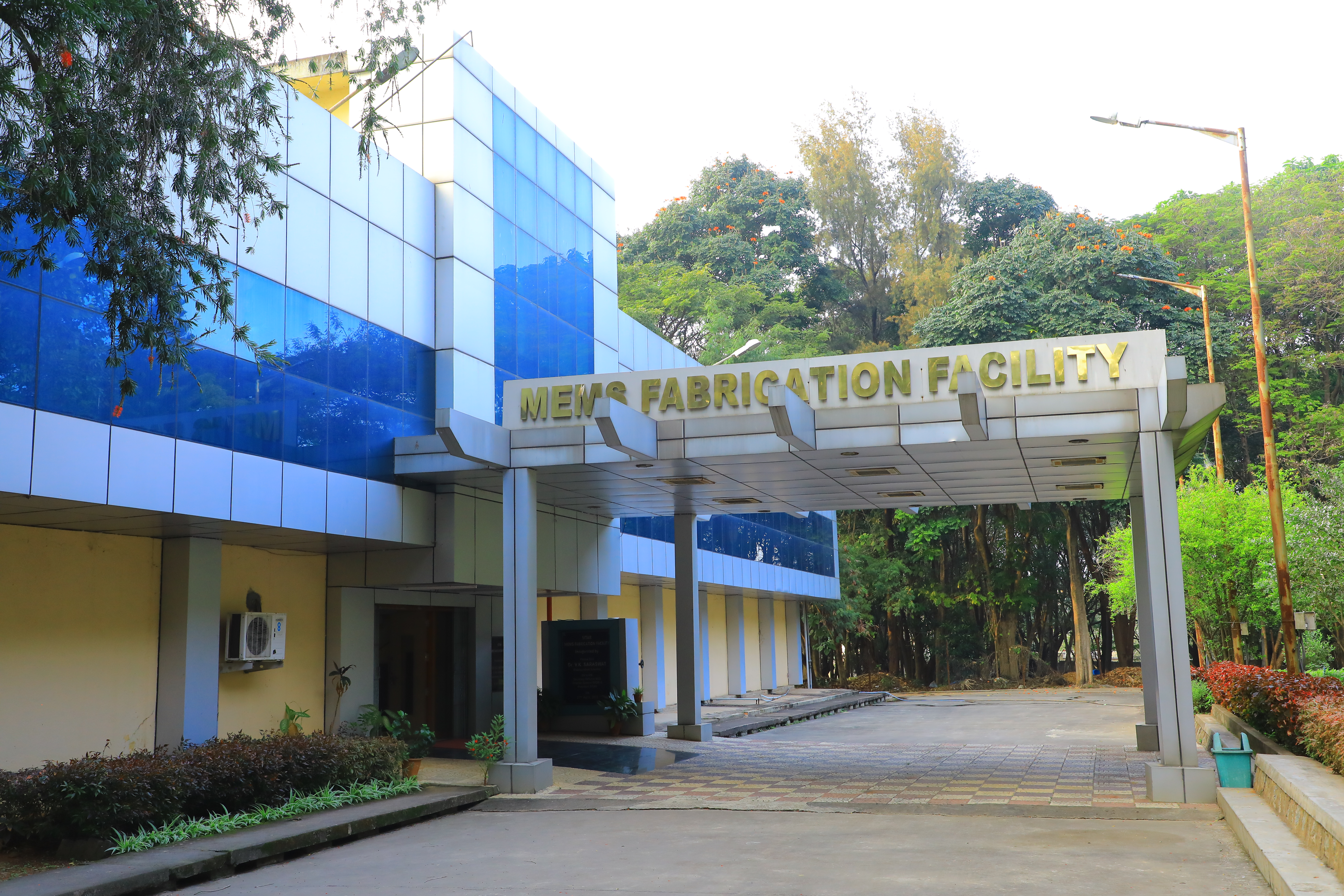
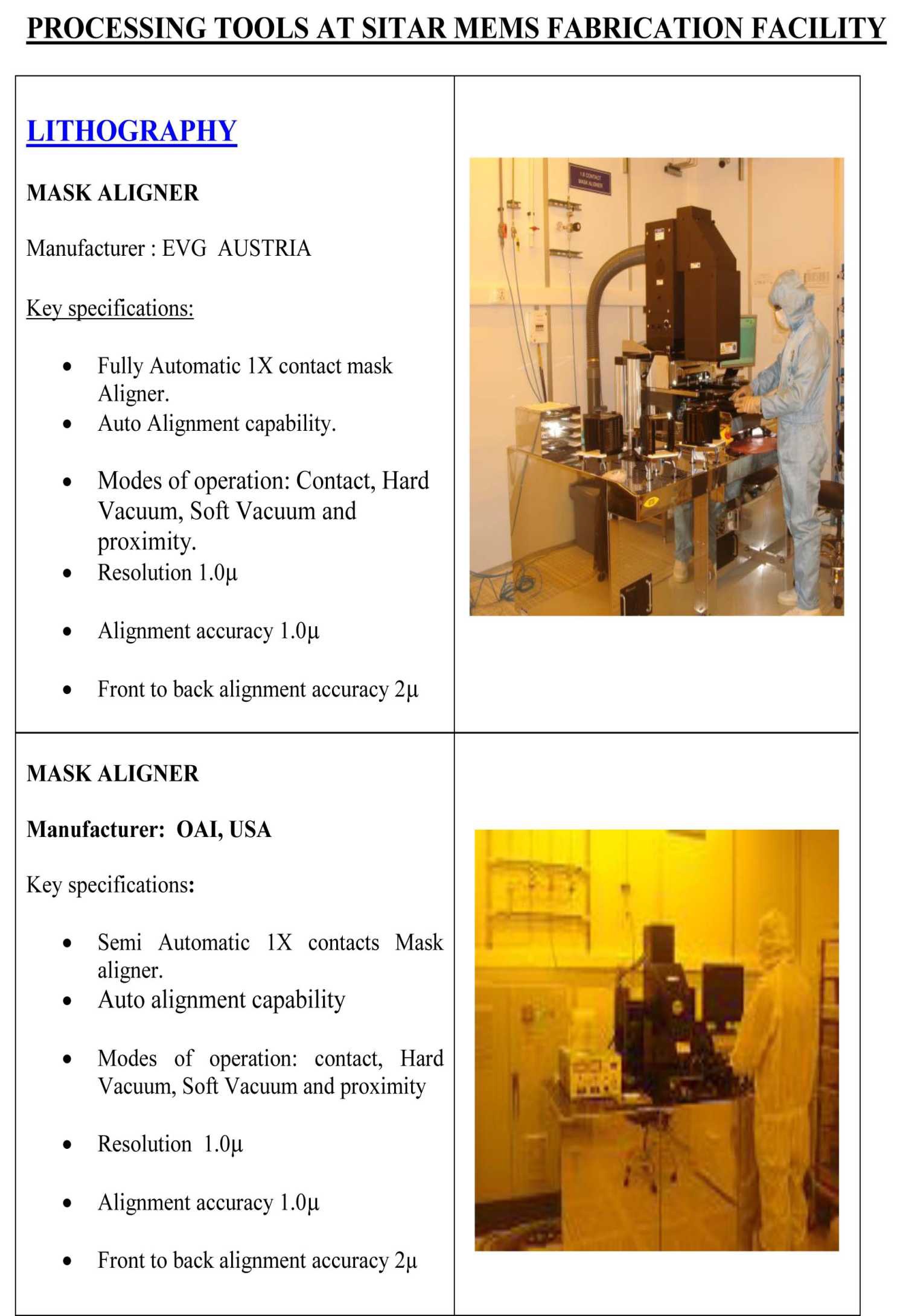
State of art MEMS fabrication facility for processing silicon 6-inch wafer with 1um feature size has been established.
Processed 6” wafers with 1µm feature size processed dies comes to A&P dept. for assembling in suitable package for easy functional and environmental testing
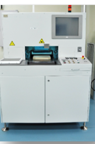
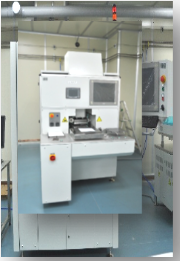
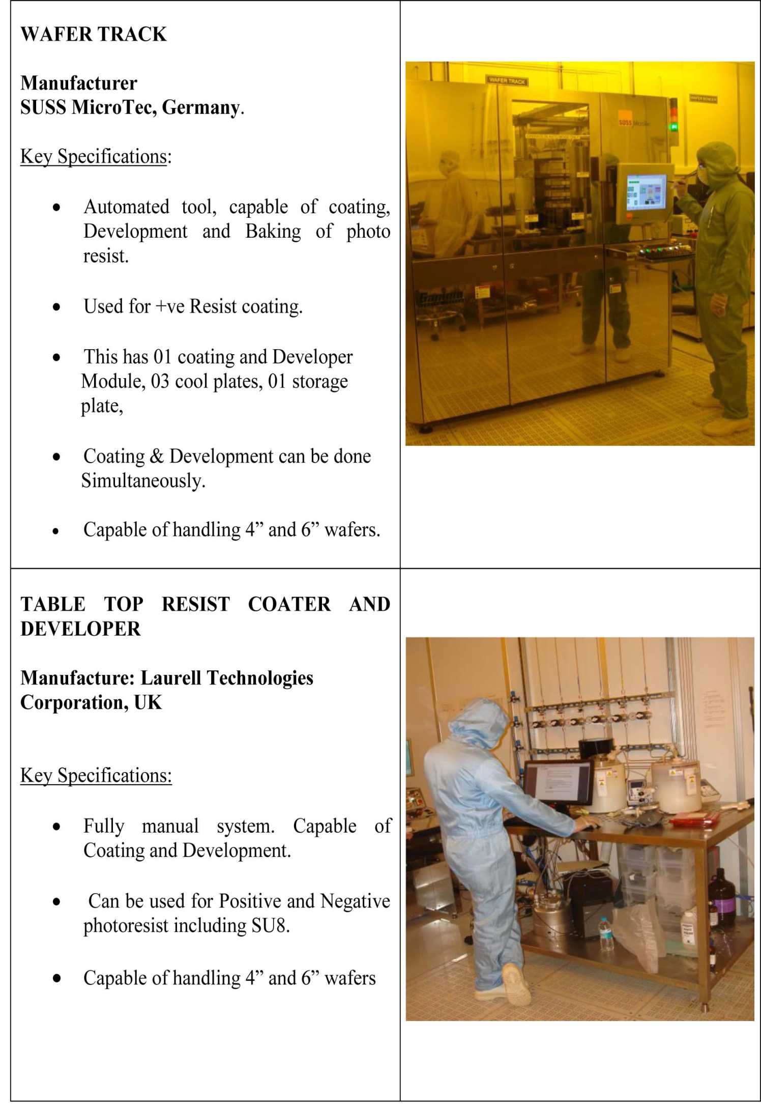
Apart from the above common equipment’s, Associated list are underneath:
Processed 6” wafers with 1µm feature size processed dies comes to A&P dept. for assembling in suitable package for easy functional and environmental testing
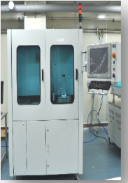
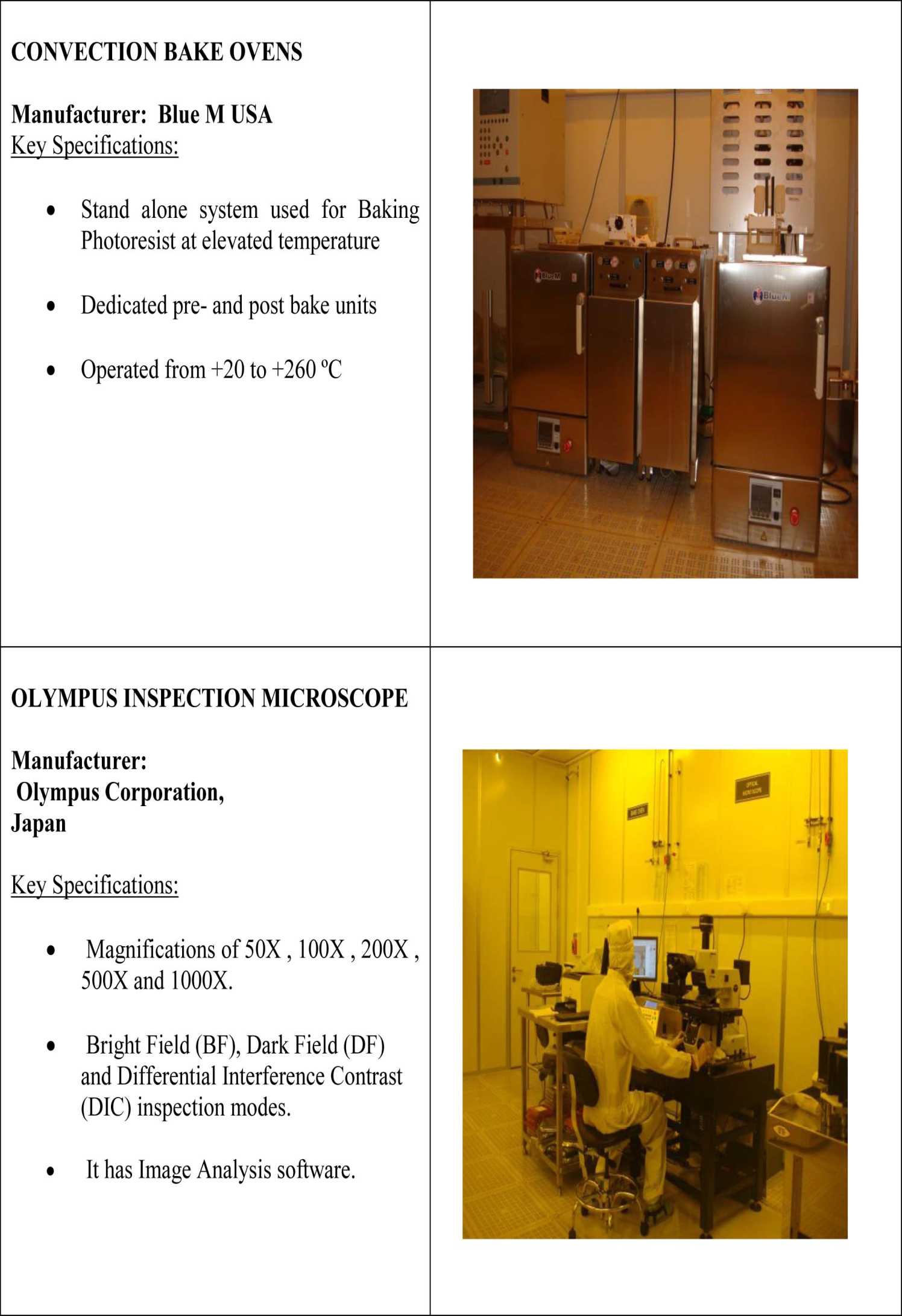
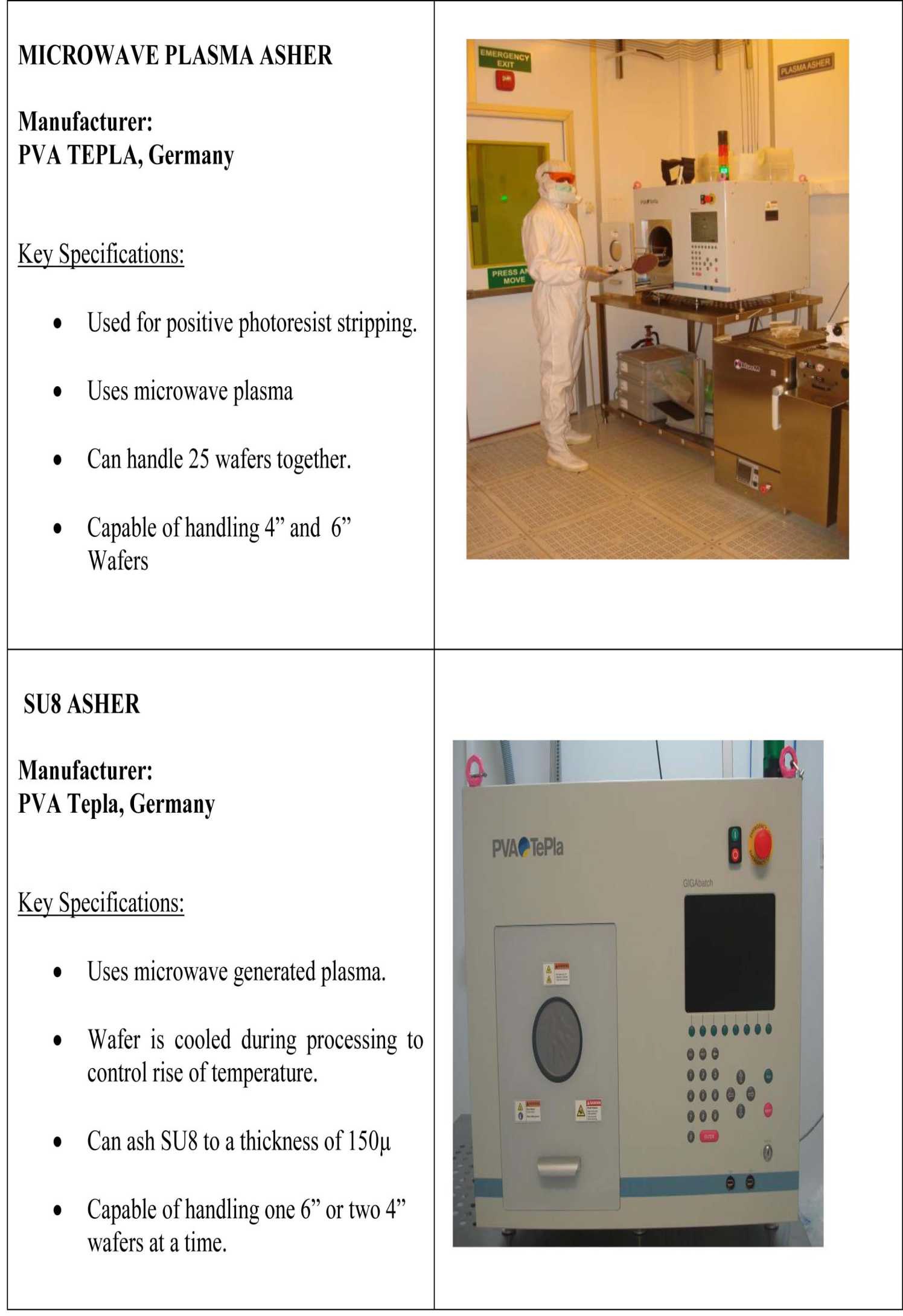
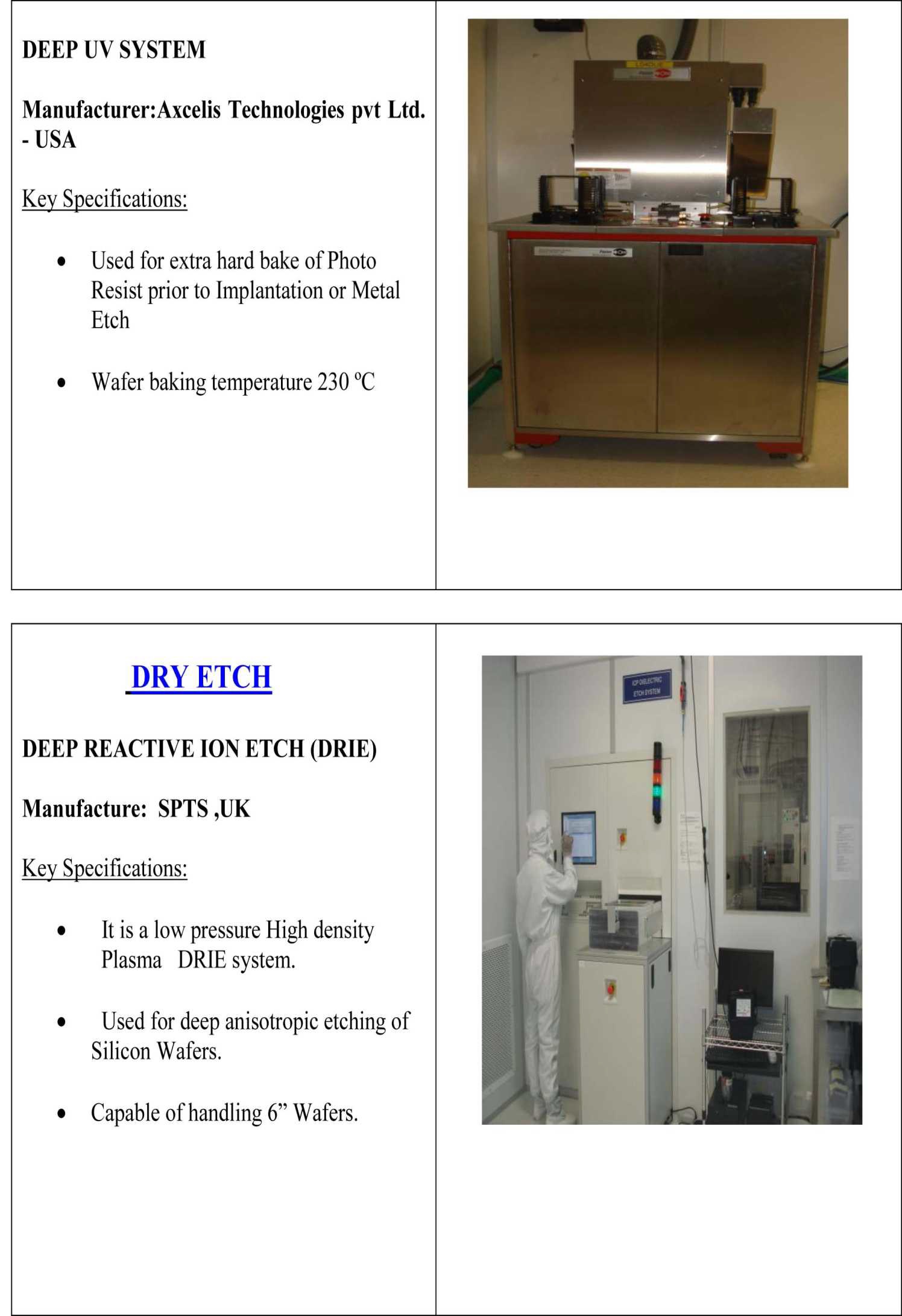
Apart from the above common equipment’s, Associated list are underneath:
State of the art fabrication facility for processing 8-inch X 8 inch ceramic substrates using Low Temperature Co-fired Ceramic (LTCC) technology has been established at STARC Bangalore for packages of MEMS Sensors and other Devices. Major process includes: Via punching, Via filling, Conductor Printing, Automated Vision Inspection, Automated Stacking, Iso static lamination, Semi automated green sheet cutting, Programmable control Co firing, Dicing.
Fabrication process is optimised for FERRO make green tapes and pastes. The process design rules are framed keeping in view of the process capability and unit process developed at STARC fabrication facility as on date.